
Electronics Inspection Optics Guide

Machine Vision Lenses for Electronics Inspection: PCB, Semiconductor, and Battery Applications

PCB AOI, wafer and die defect detection, and battery cell and pack inspection each put different demands on the lens. This guide covers low distortion for fiducial and placement geometry, adjustable iris for depth-of-field control, ground-sample-distance sizing for defect detection, longer focal length for stand-off constraints, and when telecentric optics apply.

By the Commonlands engineering team · Updated July 2026 · 19 min read

A high-magnification camera with a C-mount lens over a circuit board and silicon wafer

Electronics, semiconductor, and battery inspection are three different optical problems sharing one framework: define the smallest feature to detect, the field of view the station needs, and the working distance the fixture allows, then choose distortion, aperture, and image circle to match. Low distortion matters most for fiducial and placement geometry; adjustable iris matters most where component or cell height varies; longer focal length solves stand-off clearance in battery packs; telecentric optics apply only to the narrow slice of dimensional metrology across all three domains.

Commonlands covers these tasks with the CIL052 (5.2mm M12, low distortion) and CIL522 (12mm C-mount, adjustable iris), plus longer-focal-length and large-sensor options covered in the products section below.

One selection framework for three inspection domains

Electronics manufacturing spans three distinct imaging problems that get lumped together as "AOI" or "inspection." PCB and component assembly work is mostly flat-surface geometry with real height variation from populated parts. Semiconductor inspection covers wafer and die surfaces at much finer feature sizes, where the same defect-detection-versus-metrology split determines the lens category. Battery inspection adds a further wrinkle: mechanical clearance forces the camera away from the target in module and pack assemblies, which is a working-distance problem before it is anything else.

All three domains reduce to the same three inputs before any lens gets selected: the smallest feature or defect that must be reliably detected, the field of view the station must cover, and the working distance the fixture allows. From those, focal length follows directly from focal length = (working distance × sensor dimension) / field dimension, a rectilinear-projection relation that is accurate when the working distance is much larger than the focal length; verify close-range setups with the calculators below. Lens category (M12, C-mount, or the narrow telecentric case) comes after those numbers are set, not before.

Domain Representative task Primary optical driver Likely lens direction
Electronics / PCB Fiducial + component placement AOI Low distortion across the field 5mm M12 or 6–12mm C-mount
Electronics / PCB Solder joint / connector height Adjustable iris for depth of field C-mount with iris ring
Semiconductor Wafer surface / die defect detection Resolution, contrast, matched image circle 16–35mm C-mount, 12–20MP sensor
Semiconductor Trace width / bump height metrology Magnification constancy Telecentric (not a Commonlands product)
Battery Pouch cell / tab alignment Low distortion, flat coverage at WD 5mm M12 or 12mm C-mount
Battery Stand-off module / pack inspection Reach target from clearance distance 50mm M12 or 25mm C-mount telephoto
Shared calculators

Use the Commonlands field-of-view calculator to verify coverage from a working distance, and the EFL calculator to work backward from field of view to focal length.

Once focal length and field of view are set, check the depth-of-field calculator to confirm whether an aperture covers a given height variation before committing to a lens.

A worked resolution budget across the three domains

Ground-sample distance ties the three domains together more directly than lens category does, because it is the same calculation regardless of whether the target is a PCB, a wafer, or a battery cell. GSD equals field width divided by the sensor's active pixel count along that axis, and the practical sizing rule is to keep GSD 2 to 3 times smaller than the smallest feature that must be reliably flagged.

Consider a 5MP sensor (2592 × 1944 pixels) covering three representative fields. A 60mm wide PCB fiducial field gives a GSD of roughly 23μm per pixel, comfortable for 0.5mm BGA pitch but marginal for detecting a 50μm solder bridge without narrowing the field or increasing sensor resolution. The same sensor on a 12mm wafer inspection field gives a GSD near 4.6μm, adequate for 15–20μm surface defects but not for sub-5μm particle detection, which typically pushes toward a longer focal length, a smaller field, or a higher-resolution sensor instead. On a 60mm battery module field (the CIL051 example at 500mm working distance, covered in the battery section below), GSD is roughly 23μm, appropriate for locating a connector or weld seam but not for measuring seal gap width to a tight tolerance.

The pattern holds across all three domains: GSD is a direct function of field width and pixel count, not of mount type or focal length in isolation. Two lenses with different focal lengths that produce the same field of view on the same sensor produce the same GSD. For a fixed sensor, GSD only improves by narrowing the field of view (achieved with a longer focal length or a shorter working distance) or by moving to a higher-resolution sensor, which relaxes the fixed-sensor assumption itself.

A silicon wafer under an inspection camera, its mirror surface showing fine die patterns
High magnification resolves the fine features on a semiconductor wafer.

Does PCB AOI need a low distortion lens?

Yes, for most PCB geometry and fiducial tasks. Automated optical inspection registers a board to fiducial marks, then measures component placement relative to those references, and lens distortion displaces apparent feature position most at the field edges, exactly where many components sit.

A lens with 1% TV distortion shifts apparent feature position at the field boundary by roughly 1% of the field half-width; on a 60mm wide field that is about 0.3mm of positional error at the corners. Whether that matters depends on component pitch: 0402 passives with 1mm pads tolerate it, while fine-pitch BGA packages with 0.5mm ball pitch do not. A lens specified at 0.3% TV distortion or lower is a common target for keeping edge positional error small relative to fine-pitch spacing, though the acceptable figure depends on the component pitch, field size, and the AOI system's own tolerance rather than a single universal threshold. See what is a low-distortion lens for how distortion is specified and measured.

Code and label reading on board-mounted marks

PCBs and assemblies carry barcode, QR, or data matrix marks on printed or adhesive labels. A code near the image center decodes reliably on most lenses; the same code near the image corner on a distorted lens has compressed or stretched elements, which degrades decode confidence. Low distortion across the full field, not just at center, is the specification that prevents this failure mode on a production line reading every board.

Where distortion matters less

Solder paste coverage, surface contamination, and component presence checks by silhouette or color care about contrast and resolution, not geometric accuracy. Stopping down to improve depth of field helps these tasks more than tightening the distortion spec. Match the distortion requirement to the geometric precision the specific task needs rather than over-specifying by default.

Why does solder joint inspection put pressure on depth of field?

A populated PCB is not flat. Tall connectors, through-hole components, and uneven solder volumes create height variation across the inspection area, often several millimeters on a dense board. Depth of field at a given aperture may not cover that full range when focus is set to the board surface, which leaves tall components or connector pins soft. Stopping down (increasing the F-number) deepens depth of field roughly linearly, about 2.9x between F/2.8 and F/8, at the cost of required illumination, which scales with the square of that factor: roughly 8x more light for the same F/2.8-to-F/8 move.

In an electronics inspection station, LED illumination is typically controlled programmatically, so trading light throughput for depth of field is a routine optimization rather than a compromise. The iris ring on a C-mount lens makes that trade available in the field; a fixed-aperture M12 lens does not, so depth of field has to be engineered in at the design stage instead through working distance and focal length choice.

Connector and socket inspection

Connectors introduce their own geometry: the mating face may be recessed, and individual pins sit at slightly different heights from manufacturing variation or mating history. A lens stopped down to F/8 or F/11 covers that height range with enough resolution to detect bent or missing pins; a fixed F/2.8 lens may leave the rearmost pins out of focus.

When a fixed aperture is acceptable

For bare boards, flat substrates, or assemblies where component height is small and controlled, fixed aperture works fine. M12 lens apertures are chosen to balance resolution and depth of field for their intended field of view at the design stage. The constraint only becomes a problem once height variation exceeds what that fixed aperture provides. Verify the depth-of-field requirement with the Commonlands depth-of-field calculator before committing to a fixed-aperture design on a board with tall components.

When does C-mount earn its size penalty in electronics inspection?

C-mount lenses are physically larger and heavier than M12 lenses. The advantages are adjustable iris, larger image circles, and consistent optical quality across a wider sensor area. In electronics inspection, those advantages earn their size and cost in three recurring situations.

Large sensors and high pixel counts

A 20MP sensor with a 1.1-inch image circle captures more information per frame than a 5MP sensor on a smaller format, but only if the lens image circle actually covers that sensor. A lens designed for a 2/3-inch image circle placed in front of a 1.1-inch sensor vignettes and loses corner sharpness outside its design circle. The CIL544 25mm C-mount has a 17.6mm image circle specifically to serve 1.1-inch, 20MP+ sensors; matching image circle to sensor format is the first check before evaluating any other specification.

Tuning margin across product changeovers

A station that runs multiple board types with different heights and working distances benefits from independently adjustable iris and focus. C-mount lenses provide that margin because both are mechanical rings on the lens body. An M12 lens is optimized for one configuration; a product changeover that shifts depth-of-field or focus-plane requirements means physically repositioning the lens in its holder rather than turning a ring.

This matters on lines that run mixed board lots with different component heights. A line alternating between a thin single-layer board and a thicker multilayer board with taller connectors can re-tune depth of field on a C-mount lens by turning the iris ring, whereas the same change on a fixed-aperture M12 lens generally requires repositioning the lens in its holder or swapping optics. Whether that difference is significant depends on the line's own changeover and re-qualification requirements.

Wider fields at a moderate cost

Shorter focal length C-mount lenses combined with an adjustable iris cover a full PCB panel or a wide inspection zone in one frame while still allowing aperture control, an advantage a fixed-aperture alternative at the same field of view does not have. Browse the full C-mount lens catalog for current focal length options.

When does M12 still make sense for electronics inspection?

M12 lenses are compact, light, and integrate directly into many embedded camera modules. M12 is the right default when the inspection head must fit inside a tight fixture and the sensor is 1/1.8 inch or smaller.

Compact inline inspection heads

Pick-and-place machines, label applicators, and inline PCB conveyors often integrate the inspection camera into the machine body, where the camera-and-lens assembly must fit within a mechanical envelope that rules out the larger diameter of C-mount optics. The CIL052 5.2mm M12 lens, at −0.1% distortion and covering up to 1/1.8-inch sensors, fits inside a compact housing while still delivering the low distortion that fiducial and code-reading tasks need.

A fixed aperture is acceptable in many AOI setups

If the board under inspection has limited height variation and the task is presence, polarity, or code reading on a flat or near-flat surface, fixed aperture is not a constraint. The M12 lens aperture can be matched to working distance and required depth of field at the design stage. Most bare-board AOI, pre-reflow solder paste inspection, and pre-assembly label reading fall into this category.

The practical limit of M12

M12 lenses currently top out around 1/1.7-inch sensor coverage. A station that needs a 2/3-inch or larger sensor for resolution, dynamic range, or low-noise imaging requires C-mount optics. The larger image circle is a physical constraint, not a preference. Any station where depth-of-field adjustment during production is a requirement also needs iris control, which M12 lenses generally do not provide. See the M12 lens catalog for current options.

Choosing a machine vision lens for semiconductor inspection

Semiconductor inspection covers wafer surface screening for particle contamination and process defects, die inspection of bond pads and alignment marks at higher magnification, and package inspection of solder ball geometry or lead coplanarity. Each starts from the same three inputs as electronics inspection generally (smallest feature to detect, field of view, working distance), but the feature sizes are typically an order of magnitude finer, which pushes the resolution and distortion budgets tighter.

The task splits cleanly into two categories with different optical requirements. Defect detection flags anomalies (particles, scratches, voids, cracks) and does not need the image to represent physical dimensions accurately; distortion in the 0.3–0.5% range is typically tolerable because contrast and resolution, not geometry, drive detection accuracy. Dimensional metrology measures trace width, die placement offset, or bump height to a tolerance, which requires distortion below 0.1% and, for tight critical-dimension work, below 0.05%.

At 0.1% distortion over a 10mm field width, the worst-case positional error at the field edge works out to 5μm. Whether that is acceptable depends entirely on the measurement tolerance the station is designed against.

Semiconductor task Optical priority Likely lens direction
Wafer surface AOI Resolution, contrast, uniformity C-mount, low distortion, matched image circle
Die defect detection High resolution, low distortion 16–35mm C-mount, 12–20MP sensor
Bond pad alignment verification Low distortion, stable magnification C-mount at <0.1% distortion
Critical dimension / bump height metrology Magnification constancy, minimal perspective error Telecentric (not a Commonlands product)
Compact embedded inspection Small form factor, fixed WD M12 telephoto (constrained stations only)

Ground-sample distance (GSD), the physical size a single pixel represents at the object plane, is the sizing tool for resolution. Divide field width by pixel count across that axis; for reliable defect detection the GSD should be 2 to 3 times smaller than the minimum feature. A 12MP sensor (4000 × 3000 pixels) imaging a 12mm wide field gives a GSD of roughly 3μm per pixel, comfortable for 10–30μm surface defects but insufficient for reliably detecting 2μm particles without narrowing the field, increasing sensor format, or decreasing pixel pitch. The CIL533 and CIL535 are specified at −0.1% distortion, within range for AOI and alignment verification and at the edge of what is usable for tight metrology work.

The CIL545 tightens that budget further, at −0.07% distortion, for stations closer to the tight-metrology edge of that range.

Longer focal lengths used at longer working distances also narrow the range of viewing angles across the field, which can reduce position-dependent specular glare on reflective wafers and metallic packages depending on the illumination geometry, a practical reason to prefer a longer lens from further back when the field-of-view math would allow either. See how to choose focal length for machine vision for the full sizing sequence and spatial resolution in machine vision for GSD and minimum-detectable-size fundamentals.

Choosing a machine vision lens for battery inspection

Battery inspection spans pouch cell and prismatic case surface inspection, cylindrical cell code reading, weld and seal verification at cell tabs, and stand-off inspection of modules and packs. The first three are variations on the electronics-inspection framework above; the fourth introduces a constraint specific to battery assembly: mechanical clearance that keeps the camera away from the target.

Flat cell surfaces and code reading

Pouch cells and prismatic cases are flat, bounded targets viewed roughly overhead, so the same low-distortion logic that applies to PCB fiducials applies here: barrel distortion bows straight cell edges outward while shifting point features like tab positions radially inward toward center, and a lens at 0.5% or less distortion keeps that geometry trustworthy without software correction. Data matrix and barcode marks on cylindrical cells or flat labels have the same requirement: distortion compresses or stretches symbol spacing at the field edge, which degrades decode reliability. Weld and seal inspection is the exception: it cares about contrast and resolution at the weld zone more than geometric accuracy, since coaxial or structured illumination revealing bead texture or seal gap is the driving factor, not position measurement.

Why stand-off inspection needs a longer focal length

Battery module and pack assemblies have thermal management components, structural members, and wiring that block close camera placement, often forcing the camera outside a 200mm to 500mm exclusion zone. A longer focal length achieves a narrow field of view from that distance without wide-angle distortion or an awkward camera angle. At 500mm working distance, a 50mm M12 lens such as the CIL051 (7.5mm image circle, per its published field-of-view specification) covers roughly 60mm of field width on a 4:3 sensor, useful for a connector, alignment feature, or localized mark. The same sensor with a 12mm lens at the same distance covers roughly 250mm, too wide for a localized check and requiring the camera further outside the available fixture space. This is a geometry constraint solved by a standard telephoto lens, not an exotic optical requirement; see machine vision lens for long working distance for the full telephoto selection process.

When a telephoto lens is not the right fix

A longer focal length narrows field of view. If the task is covering a full module surface rather than a localized feature, a single telephoto camera may not be the right approach. Multiple cameras at shorter focal lengths, or a scanning approach, is often more practical. Working distance and coverage area are interdependent; neither is optimized independently of the other.

C-mount and M12 tradeoffs for battery stations

C-mount earns its size penalty in battery inspection under the same conditions as electronics inspection generally: adjustable iris for uneven weld beads or stacked-cell height variation, sensors larger than 1/1.8 inch, or tuning margin across multiple cell formats. M12 remains the better default for compact, embedded, or cost-sensitive setups where the sensor is 1/1.8 inch or smaller. Neither mount is inherently better here. The specific need for iris control or larger sensor coverage determines which one earns its tradeoffs on a given station.

When a telecentric lens is justified across all three domains

Object-space telecentric lenses keep the chief ray close to parallel with the optical axis in object space (the entrance pupil sits at infinity), which means an object's apparent size stays effectively constant as its distance from the lens varies within the depth of field. That property matters only when a measurement's accuracy depends on it; it does not matter for pass/fail detection tasks.

The genuine use case is dimensional metrology

Trace width, pad pitch, bump height, tab spacing, and lead coplanarity all require that a pixel position correspond to a known physical position regardless of small height variation in the target. With a standard entocentric lens, a 1mm height change at 200mm working distance with a 12mm focal length shifts apparent magnification by roughly 0.5%, which is a 0.025mm apparent position error at the edge of a 10mm field. Whether that is significant depends on the measurement tolerance; for a ±0.1mm tolerance it is not negligible. Telecentric optics remove that sensitivity within their depth of field, which is why they earn their cost specifically for this narrow class of measurement tasks across PCB, semiconductor, and battery inspection alike.

Where a telecentric lens is not the right answer

Telecentric lenses require a front aperture at least as large as the object field, so a lens covering a 50mm inspection zone is at least 50mm in diameter at the front element. That size constrains fixture design and creates clearance problems in automated assembly equipment, and cost is significantly higher than a comparable-resolution C-mount lens. PCB AOI, wafer and die defect detection, code reading, weld inspection, and pouch-cell surface checks are pass/fail tasks that do not need magnification constancy. They need adequate resolution, contrast, and depth of field, which a well-specified C-mount lens with sub-0.5% distortion provides at a fraction of the cost and without the fixture-clearance penalty.

Commonlands product scope

Commonlands does not currently offer telecentric lenses. For dimensional metrology tasks that genuinely require them, verify the object-field size and depth-of-field specification against the measurement tolerance budget before committing to a telecentric design. Most electronics, semiconductor, and battery inspection tasks do not clear that bar. See what is a telecentric lens for the underlying optics and lenses for quality inspection for the broader inspection-hub framework this pillar sits under.

Top machine vision lenses for electronics inspection

For PCB, semiconductor, and battery inspection, Commonlands covers the pass/fail and low-distortion measurement tiers with fixed-focal-length lenses ranked by task below. The CIL052 (5.2mm M12, −0.1% distortion) handles PCB fiducial and code work, the CIL522 (12mm C-mount, F/1.4–F/16 iris) covers solder and connector depth of field, and longer C-mount and telephoto options serve wafer, die, large-sensor, and stand-off battery stations. Each has published distortion and image circle specifications; none has autofocus or image stabilization.

Inspection domain Lens Mount EFL Why this pick
PCB fiducial + placement AOI CIL052 M12 5.2mm −0.1% distortion holds component positions across the field; 70° FoV at a 7.2mm circle, and the 9.0mm as-designed circle covers up to 1/1.8″ sensors in a compact head.
Solder joint + connector inspection CIL522 C-mount 12mm F/1.4–F/16 adjustable iris trades light for depth of field across board height variation; 51° FoV at an 11mm image circle for 2/3″ sensors.
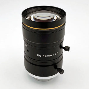
Wafer surface + substrate AOI CIL533 C-mount 16mm −0.1% distortion and an 11mm image circle for 2/3″ 12MP sensors; resolution and uniformity for surface defect screening.
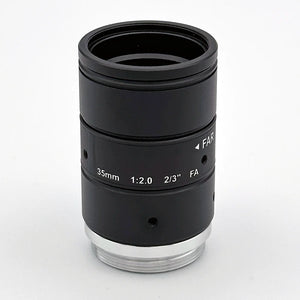
Die inspection + alignment CIL535 / CIL545 C-mount 35mm Narrower 18° field for higher magnification at longer working distance; CIL535 at −0.1% distortion, CIL545 at −0.07% for the tighter-distortion edge of metrology work.
Large-sensor 20MP+ inspection CIL544 C-mount 25mm 17.6mm image circle covers 1.1″ 20MP+ sensors; F/1.8 adjustable iris and 130mm–∞ working distance.
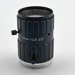
Battery module + pack stand-off CIL051 M12 50mm 9° FoV reaches the target from a 200–500mm clearance zone at 18g; 0.1% TV distortion on a 7.5mm image circle.
Board-mark code reading CIL052 M12 5.2mm Low distortion keeps data matrix and barcode elements decodable at the field corners, not just at center.

Flat pouch-cell surface and label code reading reuse the low-distortion CIL052 or CIL522 picks; the stand-off row covers battery module and pack clearance, where reach is the binding constraint. For tight dimensional metrology, a telecentric lens is the right tool, and telecentric lenses are third-party products rather than Commonlands SKUs.

How we picked

Each row matches the domain's primary optical driver to the lens spec that satisfies it: distortion for geometry-sensitive PCB and wafer work, adjustable iris for height-varying solder and connector stations, image circle for large-sensor resolution, and focal length for stand-off reach. Rankings use only published distortion, image circle, and field-of-view figures from the product pages, with no interpolated sensor math. Confirm coverage on your own sensor with the field-of-view calculator and depth of field with the depth-of-field calculator before ordering.

A low-distortion C-mount lens inspecting fine-pitch solder joints across a circuit board
Low distortion keeps solder joints sharp and true across the frame.

Frequently asked questions

What lens should I use for electronics inspection in machine vision?

Start with the inspection task, not the lens family. PCB AOI and fiducial checks need low distortion so component positions read correctly across the field. Solder joint and connector inspection needs adjustable iris for depth-of-field control across board height variation. High-resolution stations need a lens image circle matched to the sensor. Commonlands options include the CIL052 (5.2mm M12, low distortion), CIL522 (12mm C-mount, adjustable iris), and CIL544 (25mm C-mount, large-sensor inspection).

Does PCB AOI need a low distortion lens?

Yes, for most PCB geometry and fiducial tasks. AOI systems measure component position relative to fiducial marks, and distortion displaces apparent positions near the field edges. A lens at 0.3% TV distortion or lower is a common target for keeping edge positional error small relative to fine-pitch BGA spacing, though the acceptable figure depends on component pitch, field size, and the AOI system's own tolerance rather than a single universal threshold. Contrast-only tasks such as solder paste coverage are less sensitive to distortion. See what is a low-distortion lens for the full explanation.

Does semiconductor inspection require a telecentric lens?

No, not for every application. Telecentric optics are justified when perspective error would corrupt a dimensional measurement or when magnification must stay constant despite part height variation, such as trace-width or bump-height metrology. For flat-surface wafer and die defect detection, a standard C-mount lens with sub-0.5% distortion and an adjustable iris is typically sufficient and far less expensive. Commonlands does not currently sell telecentric lenses.

How much distortion is acceptable for wafer or die inspection?

It depends on whether the task is defect detection or dimensional metrology. Defect detection tolerates distortion of 0.3–0.5% or more since the goal is flagging anomalies, not measuring geometry. Dimensional metrology needs distortion below 0.1%, and ideally below 0.05% for tight critical-dimension work. Commonlands C-mount lenses such as the CIL535 (−0.1% distortion) and CIL545 (−0.07% distortion) sit within range for most AOI and alignment tasks.

Does battery inspection need a low distortion lens?

It depends on the task. Flat geometry work such as pouch cell surface inspection, tab alignment, and code reading on flat labels benefits from low distortion because geometric error accumulates at cell edges and corners. Weld and seal inspection cares more about contrast and resolution than geometric accuracy. Stand-off module inspection with a longer telephoto focal length typically has low distortion, so it is rarely the limiting factor there, though this varies by lens: the 50mm CIL051 runs 0.1% distortion, while the 25mm CIL544 runs closer to 1% at minimum object distance.

Why does stand-off battery inspection need a longer focal length?

Battery module and pack assemblies have mechanical clearances, thermal management components, and structural members that keep the camera away from the target. A longer focal length, typically 25mm to 50mm in M12 or C-mount format, achieves a narrow field of view from a greater working distance without wide-angle distortion or an awkward camera position. It is a geometry constraint solved by standard telephoto optics, not an exotic optical requirement. See machine vision lens for long working distance for the full selection guide.

Why does solder joint inspection put pressure on depth of field?

A populated PCB is not flat. Tall connectors, through-hole components, and uneven solder volumes create height variation across the inspection area, often several millimeters on a dense board. The depth of field at a wide aperture may not cover that range when focus is set to the board surface. Stopping down deepens depth of field at the cost of light, which is manageable because illumination is typically programmatic. Most C-mount lenses offer an adjustable iris for this; M12 lenses typically do not provide an adjustable iris. Use the depth-of-field calculator to check coverage before committing to a fixed-aperture design.

When does C-mount earn its size penalty in electronics inspection?

C-mount earns its size penalty when the station needs adjustable iris for depth-of-field control, uses a sensor larger than 1/1.8 inch, or requires an image circle matched to a 12MP or 20MP+ sensor. AOI stations moving to higher-resolution sensors need that larger image circle or corner sharpness degrades and edge defects are missed. The CIL544 25mm C-mount covers a 17.6mm image circle for 20MP+ sensors. M12 remains the right default when package size is the binding constraint and the sensor is 1/1.8 inch or smaller. Browse the full C-mount lens catalog for the current range.

When does M12 still make sense for electronics inspection?

M12 is appropriate when the inspection head must fit inside a compact fixture, the sensor is 1/1.8 inch or smaller, and fixed aperture is acceptable. The CIL052 5.2mm M12 with −0.1% distortion handles wide-field AOI and code reading in a compact body. The practical limit of M12 is fixed aperture and roughly 1/1.7-inch maximum sensor coverage. See the full M12 lens catalog for available options.

Are telecentric optics required for PCB, semiconductor, or battery inspection?

No, not for most tasks across any of the three domains. Telecentric lenses suppress perspective error and hold magnification nearly constant across height variation within their depth of field, which matters only for dimensional metrology: trace width, pad pitch, bump height, or tab spacing measured to a tight tolerance. PCB AOI, wafer and die defect detection, weld inspection, and code reading are pass/fail tasks that need adequate resolution, low distortion, and enough depth of field, all covered by standard C-mount or M12 optics. Commonlands does not currently offer telecentric lenses.

How do I choose focal length for an electronics inspection station?

Use focal length = (working distance × sensor dimension) / field dimension, a rectilinear-projection relation that is accurate when the working distance is much larger than the focal length. At a 200mm working distance with a 7.2mm sensor width and a 100mm wide inspection area, the required focal length is (200 × 7.2) / 100 = 14.4mm, making a 12mm lens the likely candidate with margin, or a 16mm lens only if the working distance can extend to roughly 225mm. Verify coverage with the Commonlands field-of-view calculator and work backward from field of view with the EFL calculator before ordering.

What resolution is needed for electronics, semiconductor, or battery inspection?

Resolution is set by the smallest feature that must be reliably detected, not by a general megapixel target. Divide the field width by the sensor pixel count to get the ground-sample distance, then size that GSD to 2 to 3 times smaller than the minimum defect or feature for reliable detection, or smaller than the measurement tolerance for dimensional work. Five to ten pixels across the narrowest bar element is a practical starting point for barcode and data matrix reading. See spatial resolution in machine vision for the full sizing method.

Need help selecting a lens for an inspection station?

Send your working distance, sensor format, and inspection task (PCB, wafer, die, or battery cell and pack) to the Commonlands engineering team. We will confirm distortion, iris, and image circle requirements and recommend the right optic. Our lenses are MTF characterized, and orders placed before 12 PM PST ship the same day.